02 / TIA LITERATURE
Low-power and Small-area Transimpedance Amplifier with Active Inductor in 65 nm CMOS
若 PDF 预览未显示,可使用上方链接打开原文。
作者与单位: 见论文原文首页(下方已附前三页原图)
会议: IEEE APCCAS 2024
DOI: https://doi.org/10.1109/APCCAS62602.2024.10808573
原文: paper.pdf
核心参考量
| 维度 | 信息 |
|---|---|
| 应用场景 | 25 Gb/s高速光通信接收机 |
| 是否实测 | 否 |
| 工艺节点 | 65 |
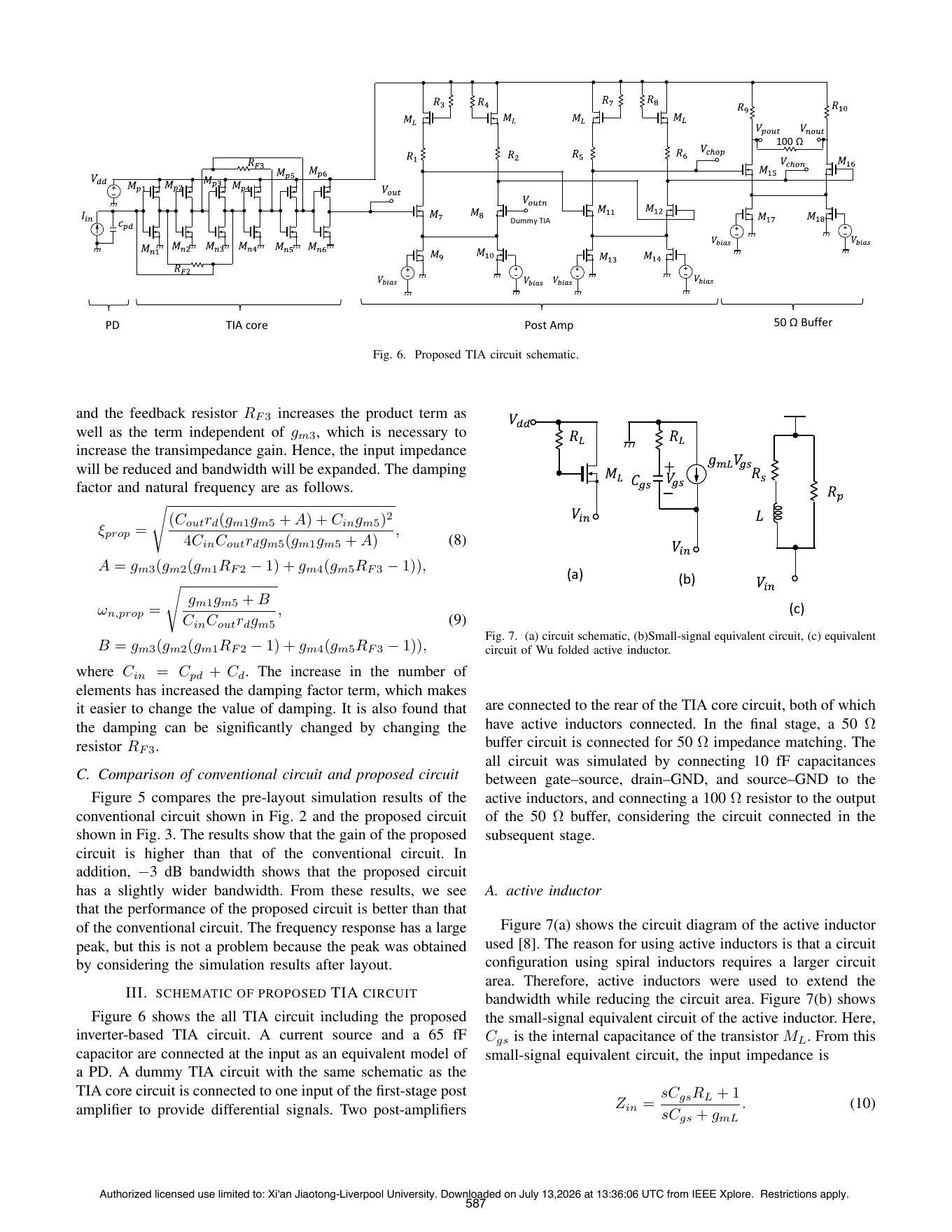
| 前端架构 | Inverter-based AVCF-TIA core + dummy TIA + two post-amplifiers with active inductors + 50 Ω buffer |
| 关键性能条件 | Post-layout;25 Gb/s PRBS-7;20 ps rise/fall;474 mVppd输出、303 mVppd眼高 |
| 可参考程度 | ★★★☆☆ |
设计挑战
- 应用约束:25 Gb/s高速光通信接收机。
- 核心电路矛盾:传统宽带TIA若依赖片外/无源电感,面积和集成成本高。本文用反相器反馈、dummy TIA与有源电感peaking在片上获得宽带和小面积;代价是高速接口导向且只有后仿。
- 指标与实现约束:Post-layout;25 Gb/s PRBS-7;20 ps rise/fall;474 mVppd输出、303 mVppd眼高。这些数值必须同时结合输入电容、输出负载、供电与验证频率判断,不能只比较单个峰值指标。
架构创新点
1. 前端拓扑
Inverter-based AVCF-TIA core + dummy TIA + two post-amplifiers with active inductors + 50 Ω buffer。该拓扑决定输入阻抗、反馈环路和主要噪声源,也是判断能否迁移到阵列读出的第一层依据。
2. 关键机制
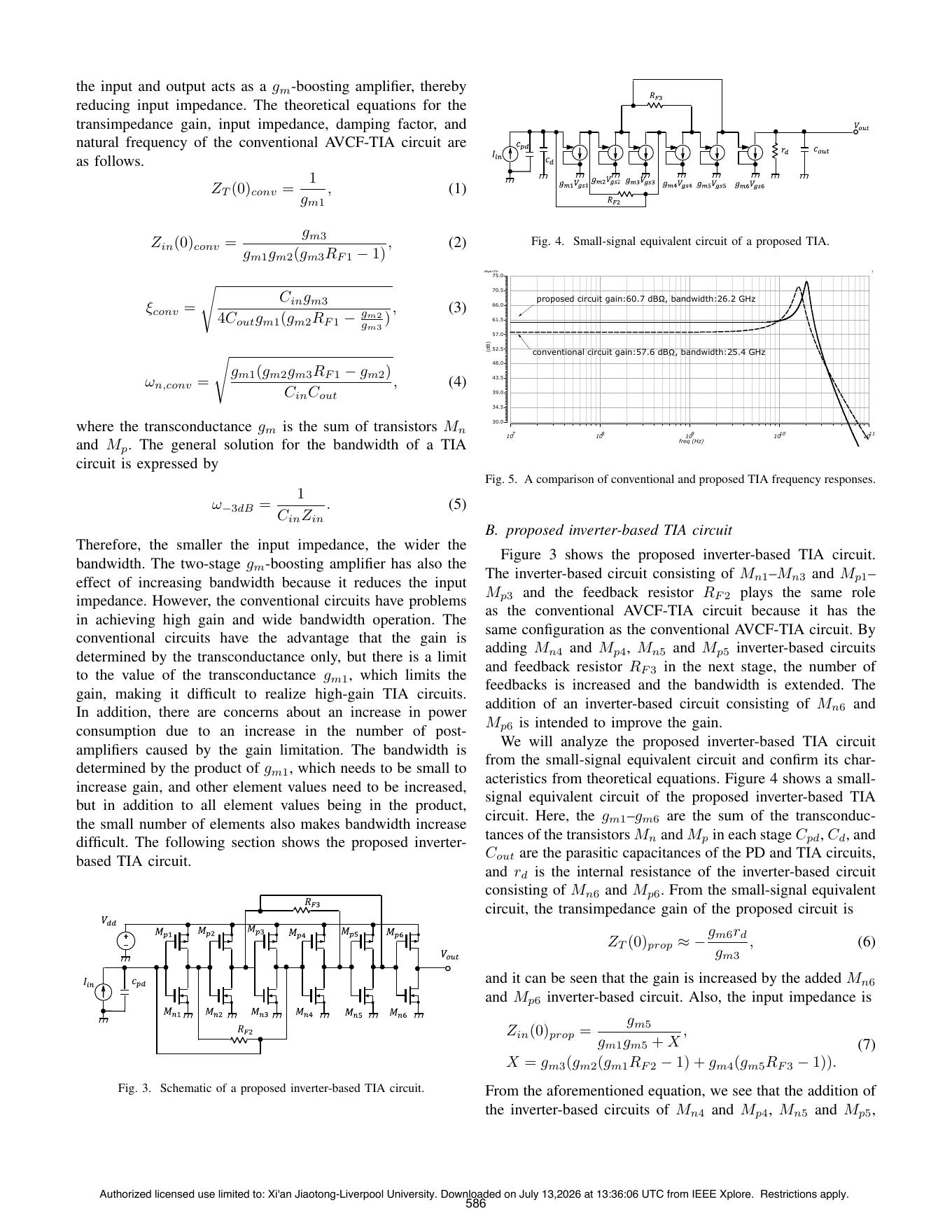
增加反馈级降低Zin并扩带;增加inverter级提高增益;active inductor实现peaking并缩小面积
3. 与传统方案的差异
传统宽带TIA若依赖片外/无源电感,面积和集成成本高。本文用反相器反馈、dummy TIA与有源电感peaking在片上获得宽带和小面积;代价是高速接口导向且只有后仿。
性能与证据
| 项目 | 判断 |
|---|---|
| 工艺 | 65 |
| 验证方式 | 否 |
| 关键性能 | Post-layout;25 Gb/s PRBS-7;20 ps rise/fall;474 mVppd输出、303 mVppd眼高 |
| 证据等级 | 仿真或后仿,证据等级中等 |
| 参考程度 | ★★★☆☆ |
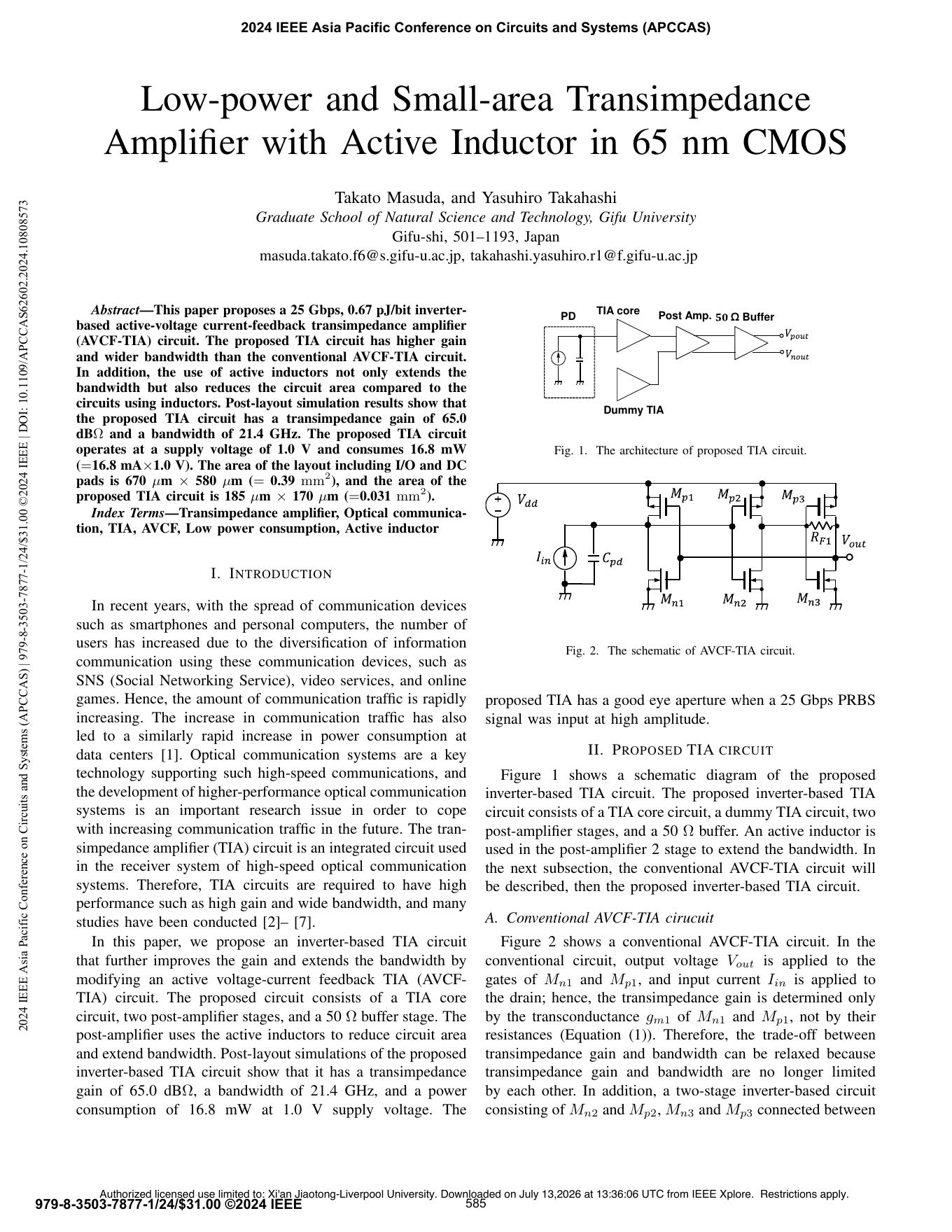
原文摘要证据:This paper proposes a 25 Gbps, 0.67 pJ/bit inverter- PD TIA core Post Amp. ȍ Buffer based active-voltage current-feedback transimpedance amplifier (AVCF-TIA) circuit. The proposed TIA circuit has higher gain and wider bandwidth than the conventional AVCF-TIA circuit. In addition, the use of active inductors not only extends the bandwidth but also reduces the circuit area compared to the circuits using inductors. Post-layout simulation results show that Dummy TIA the proposed TIA circuit has a transimpedance gain of 65.0 dBΩ and a bandwidth of 21.4 GHz. The proposed TIA circuit operates at a supply voltage of 1.0 V and consumes 16.8 mW Fig. 1. The architecture of proposed TIA circuit. (=16.8 mA×1.0 V). The area of the layout including I/O and DC pads is 670 µm × 580 µm (= 0.39 mm2 ), and the area of the proposed TIA circuit is 185 µm × 170 µm (=0.031 mm2 ).
与 SOTA 对比
- 比较重点:优先比较相同输入电容、相同带宽定义和相同输出负载下的增益、噪声、线性度与功耗。
- 本文优势:增加反馈级降低Zin并扩带;增加inverter级提高增益;active inductor实现peaking并缩小面积
- 主要限制:仅后仿真;无噪声/动态范围/线性度
- 口径提醒:会议论文中仿真值、后仿值和芯片实测值不可直接混排;未在正文报告的指标不作推算排名。
NS-RAM / CIM 适配判断
可参考低Zin和有源peaking的集成方式;NS-RAM若目标带宽远低于GHz,应避免为带宽付出不必要的功耗。
迁移到 NS-RAM 时仍需重新确定列线电容、最小/最大读电流、允许建立时间、输出摆幅和 ADC 满量程,并据此重算反馈元件与环路稳定性。
核心优势与局限
核心优势:增加反馈级降低Zin并扩带;增加inverter级提高增益;active inductor实现peaking并缩小面积
主要局限:仅后仿真;无噪声/动态范围/线性度
结论:该文适合作为“Inverter-based AVCF-TIA core + dummy TIA + two post-amplifiers with active inductors + 50 Ω buffer”路线的参考,但不能脱离其原始应用和负载条件直接套用指标。
论文原图