02 / TIA LITERATURE
Low-power transimpedance amplifier for near infrared spectroscopy
若 PDF 预览未显示,可使用上方链接打开原文。
作者与单位: 见论文原文首页
会议: IEEE ISCAS 2016
DOI: https://doi.org/10.1109/ISCAS.2016.7539081
核心参考量
| 维度 | 信息 |
|---|---|
| 应用场景 | FD-fNIRS photodiode receiver |
| 是否实测 | 否 |
| 工艺节点 | 130 |
| 前端架构 | 低输入阻抗/RGC TIA:RGC input + inverter-cascode + post amplifier |
| 关键性能条件 | TIA core 194 uW;complete receiver 2.4 mW |
| 可参考程度 | 高 |
设计挑战
- 应用约束:FD-fNIRS photodiode receiver。
- 核心电路矛盾:直接并联反馈TIA面对输入电容时带宽受限。本文以RGC降低输入阻抗,并用后级inverter-cascode提升增益;前端先解决Cin,再完成放大。
- 指标与实现约束:TIA core 194 uW;complete receiver 2.4 mW。这些数值必须同时结合输入电容、输出负载、供电与验证频率判断,不能只比较单个峰值指标。
架构创新点
1. 前端拓扑
低输入阻抗/RGC TIA:RGC input + inverter-cascode + post amplifier。该拓扑决定输入阻抗、反馈环路和主要噪声源,也是判断能否迁移到阵列读出的第一层依据。
2. 关键机制
RGC 降低输入阻抗,适合列线/输入电容适配
3. 与传统方案的差异
直接并联反馈TIA面对输入电容时带宽受限。本文以RGC降低输入阻抗,并用后级inverter-cascode提升增益;前端先解决Cin,再完成放大。
性能与证据
| 项目 | 判断 |
|---|---|
| 工艺 | 130 |
| 验证方式 | 否 |
| 关键性能 | TIA core 194 uW;complete receiver 2.4 mW |
| 证据等级 | 仿真或后仿,证据等级中等 |
| 参考程度 | 高 |
原文摘要证据:This paper presents the design and the post layout measures the time of the flight of the returned pulse [5] simulation of a high-sensitivity low-power Transimpedance making it the most expensive and complex technique. Amplifier (TIA) for frequency domain functional Near Infrared One of the advantages of NIRS is its ability to provide a Spectroscopy (FD-fNIRS). It consumes 194 µW from 1.2 V DC portable system. As a result, the system requires small chip supply. This low power will increase the battery life of the NIRS area, low power consumption and limited emitted optical portable system. The proposed TIA achieves 103.3 dBΩ power for safety. Exposure to laser is limited to a 329 mJ/cm2 transimpedance gain, 22 MHz bandwidth and 6.3 nA integrated according to American National Standards Institute (ANSI) input noise current using a photodiode with 2 pF capacitance. [6]. Accordingly, reflected optical power from tissues is The demonstra...
与 SOTA 对比
- 比较重点:优先比较相同输入电容、相同带宽定义和相同输出负载下的增益、噪声、线性度与功耗。
- 本文优势:RGC 降低输入阻抗,适合列线/输入电容适配
- 主要限制:优势:RGC、带宽、面积;短板:后仿,完整 receiver 功耗高
- 口径提醒:会议论文中仿真值、后仿值和芯片实测值不可直接混排;未在正文报告的指标不作推算排名。
NS-RAM / CIM 适配判断
适合列线/阵列端电容较大的中高速读出;需评估RGC噪声、电压余量及与NS-RAM输出偏置的兼容性。
迁移到 NS-RAM 时仍需重新确定列线电容、最小/最大读电流、允许建立时间、输出摆幅和 ADC 满量程,并据此重算反馈元件与环路稳定性。
核心优势与局限
核心优势:RGC 降低输入阻抗,适合列线/输入电容适配
主要局限:优势:RGC、带宽、面积;短板:后仿,完整 receiver 功耗高
结论:该文适合作为“低输入阻抗/RGC TIA:RGC input + inverter-cascode + post amplifier”路线的参考,但不能脱离其原始应用和负载条件直接套用指标。
电路与公式推导
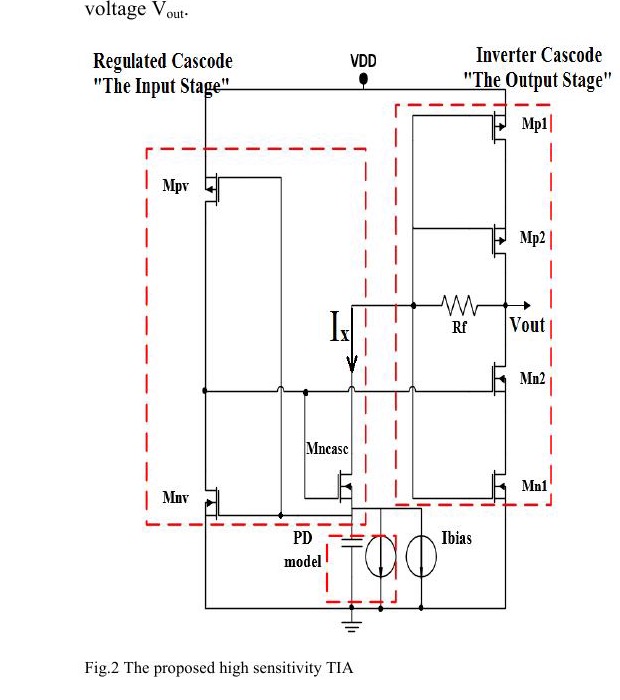
从 PD 节点 KCL 开始
令 PD 节点电压为 vx。调节反相器的增益近似为 \(A_{reg}\approx(g_{mnv}+g_{mpv})(r_{onv}\parallel r_{opv})\)。因此共栅管的局部负反馈把有效跨导提高为 \(G_{m,casc}\approx g_{m,casc}(1+A_{reg})\),当 \(A_{reg}\gg1\) 时即为论文式 (1)。
RGC 输出电流再受到级间节点 \(C_i,R_{Casc}\) 的一阶低通限制:
其中 \(R_{Casc}=(R_F+R_{out})/(A_{invc}+1)\)。高输出阻抗的 inverter-cascode 产生高 \(A_{invc}\),却通过该局部反馈使级间阻抗下降,避免形成低频主极点。
若 RGC 极点最靠近原点,带宽直接化简为 \(BW\approx G_{m,casc}/(2\pi C_{PD})\)。这就是本文以 RGC 降低输入阻抗、以级联级保持高增益的完整因果链。
原文
原文保存在私人 Obsidian 中,未公开上传。