02 / TIA LITERATURE
A CMOS Transimpedance Amplifier Accommodating Wide CPD and Input Bias Range for Chaos Lidar
若 PDF 预览未显示,可使用上方链接打开原文。
作者与单位: 见论文原文首页(下方已附前三页原图)
会议: IEEE APCCAS 2024
DOI: https://doi.org/10.1109/APCCAS62602.2024.10808803
原文: paper.pdf
核心参考量
| 维度 | 信息 |
|---|---|
| 应用场景 | Chaos LiDAR;大面积APD阵列;深度成像 |
| 是否实测 | 是 |
| 工艺节点 | 90 |
| 前端架构 | Shunt-feedback TIA + common-gate input stage + common-source second stage + CF compensation + two DC-stabilization loops |
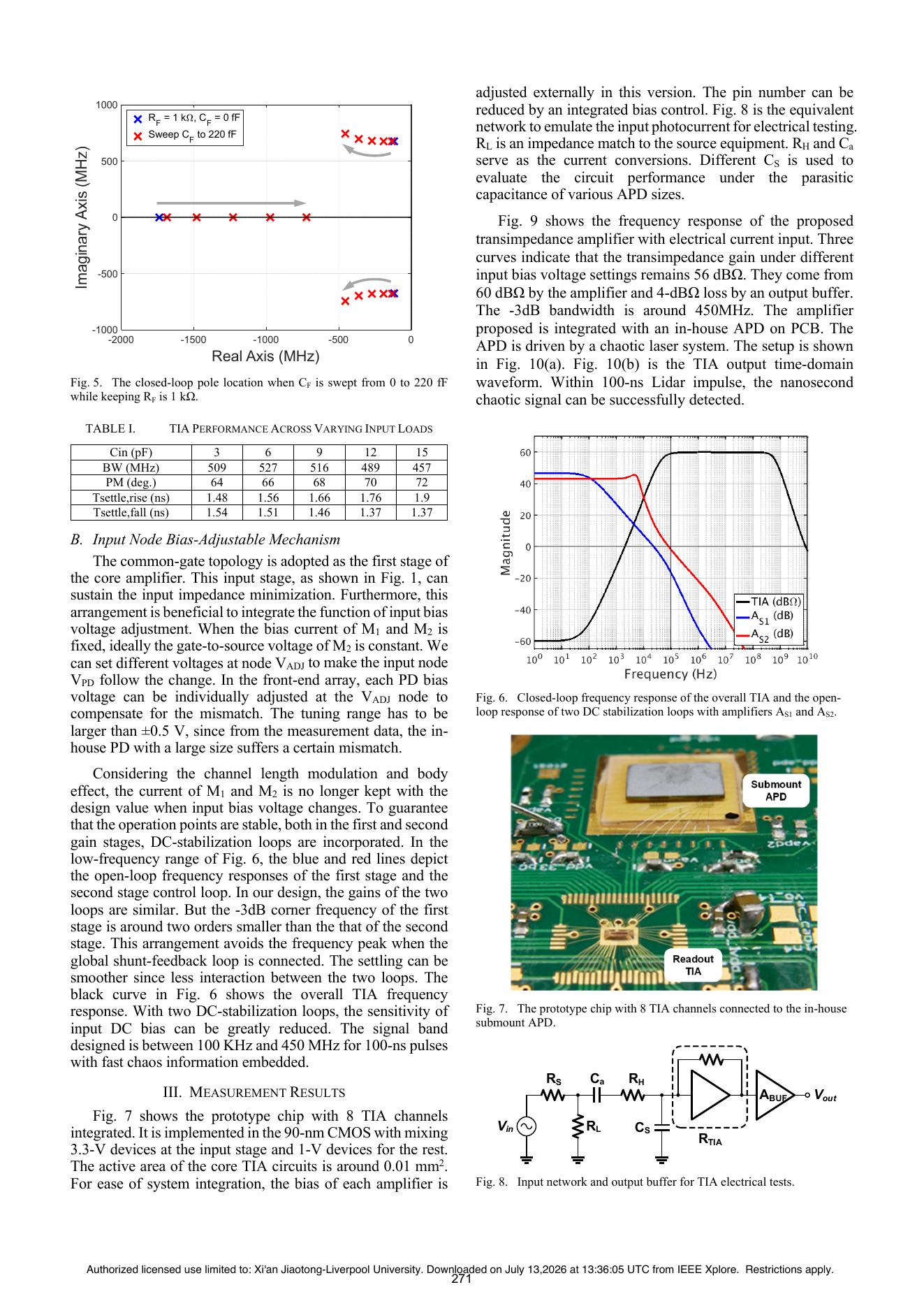
| 关键性能条件 | Cin=3/6/9/12/15 pF时BW=509/527/516/489/457 MHz;PM=64°–72° |
| 可参考程度 | ★★★★☆ |
设计挑战
- 应用约束:Chaos LiDAR;大面积APD阵列;深度成像。
- 核心电路矛盾:传统TIA遇到大光电二极管电容和输入偏置变化时带宽、稳定性易失控。本文以common-gate低输入阻抗、CF补偿和双DC稳定环把这些非理想前置处理。
- 指标与实现约束:Cin=3/6/9/12/15 pF时BW=509/527/516/489/457 MHz;PM=64°–72°。这些数值必须同时结合输入电容、输出负载、供电与验证频率判断,不能只比较单个峰值指标。
架构创新点
1. 前端拓扑
Shunt-feedback TIA + common-gate input stage + common-source second stage + CF compensation + two DC-stabilization loops。该拓扑决定输入阻抗、反馈环路和主要噪声源,也是判断能否迁移到阵列读出的第一层依据。
2. 关键机制
Common-gate降低输入阻抗;±0.5 V输入偏置调节;CF=220 fF补偿;双DC稳定环
3. 与传统方案的差异
传统TIA遇到大光电二极管电容和输入偏置变化时带宽、稳定性易失控。本文以common-gate低输入阻抗、CF补偿和双DC稳定环把这些非理想前置处理。
性能与证据
| 项目 | 判断 |
|---|---|
| 工艺 | 90 |
| 验证方式 | 是 |
| 关键性能 | Cin=3/6/9/12/15 pF时BW=509/527/516/489/457 MHz;PM=64°–72° |
| 证据等级 | 芯片实测,证据等级较高 |
| 参考程度 | ★★★★☆ |
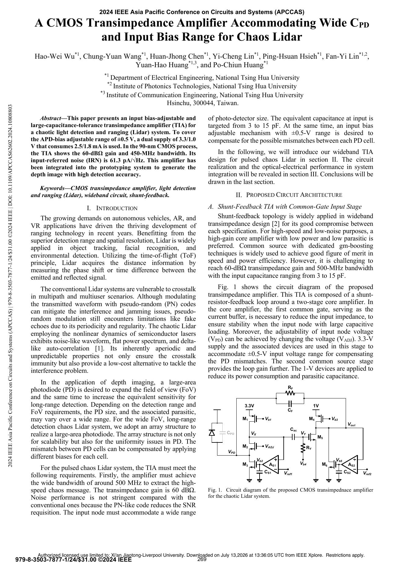
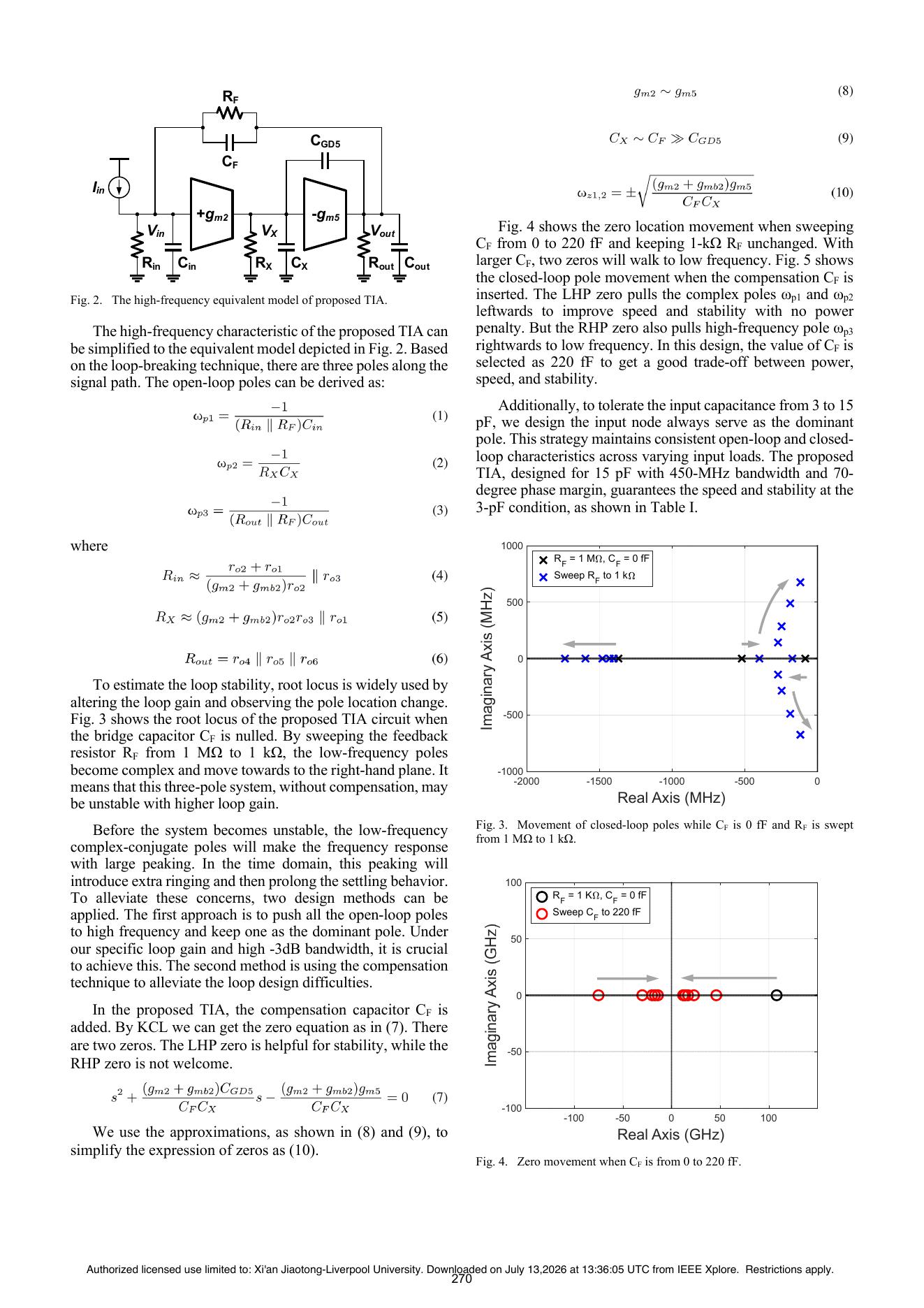
原文摘要证据:This paper presents an input bias-adjustable and of photo-detector size. The equivalent capacitance at input is large-capacitance-tolerance transimpedance amplifier (TIA) for targeted from 3 to 15 pF. At the same time, an input bias a chaotic light detection and ranging (Lidar) system. To cover adjustable mechanism with ±0.5-V range is desired to the APD-bias adjustable range of ±0.5 V, a dual supply of 3.3/1.0 compensate for the possible mismatches between each PD cell. V that consumes 2.5/1.8 mA is used. In the 90-nm CMOS process, the TIA shows the 60-dBΩ gain and 450-MHz bandwidth. Its In the following, we will introduce our wideband TIA input-referred noise (IRN) is 61.3 pA/√Hz. This amplifier has design for pulsed chaos Lidar in section II. The circuit been integrated into the prototyping system to generate the realization and the optical-electrical performance in system depth image with high detection accuracy. integration will...
与 SOTA 对比
- 比较重点:优先比较相同输入电容、相同带宽定义和相同输出负载下的增益、噪声、线性度与功耗。
- 本文优势:Common-gate降低输入阻抗;±0.5 V输入偏置调节;CF=220 fF补偿;双DC稳定环
- 主要限制:当前页面基于调研表和已下载原文建立;关键数值应以论文正文、图表和补充材料为准。
- 口径提醒:会议论文中仿真值、后仿值和芯片实测值不可直接混排;未在正文报告的指标不作推算排名。
NS-RAM / CIM 适配判断
适合大阵列Cin、偏置失配或漏电基线明显的NS-RAM;优先参考Cin扫描和相位裕度验证方法。
迁移到 NS-RAM 时仍需重新确定列线电容、最小/最大读电流、允许建立时间、输出摆幅和 ADC 满量程,并据此重算反馈元件与环路稳定性。
核心优势与局限
核心优势:Common-gate降低输入阻抗;±0.5 V输入偏置调节;CF=220 fF补偿;双DC稳定环
主要局限:当前页面基于调研表和已下载原文建立;关键数值应以论文正文、图表和补充材料为准。
结论:该文适合作为“Shunt-feedback TIA + common-gate input stage + common-source second stage + CF compensation + two DC-stabilization loops”路线的参考,但不能脱离其原始应用和负载条件直接套用指标。
论文原图