02 / TIA LITERATURE
A Dual-Mode Adjustable High-Gain Ultra-Low Noise Transimpedance Amplifier for Fine Dust Detection
若 PDF 预览未显示,可使用上方链接打开原文。
作者与单位: 见论文原文首页(下方已附前三页原图)
会议: IEEE ISCAS 2020
DOI: https://doi.org/10.1109/ISCAS45731.2020.9180567
原文: paper.pdf
核心参考量
| 维度 | 信息 |
|---|---|
| 应用场景 | Fine dust / photodiode 小电流检测 |
| 是否实测 | 否 |
| 工艺节点 | 180 |
| 前端架构 | 可调高增益低噪声 TIA:3-stage push-pull inverter + coarse/fine gain control |
| 关键性能条件 | post-layout;16-step fine gain |
| 可参考程度 | 高 |
设计挑战
- 应用约束:Fine dust / photodiode 小电流检测。
- 核心电路矛盾:传统固定反馈TIA的增益/带宽由单一Rf锁死。本文以粗细两级控制调节多级反相器TIA增益,允许在弱信号灵敏度和较大输入裕量之间切换。
- 指标与实现约束:post-layout;16-step fine gain。这些数值必须同时结合输入电容、输出负载、供电与验证频率判断,不能只比较单个峰值指标。
架构创新点
1. 前端拓扑
可调高增益低噪声 TIA:3-stage push-pull inverter + coarse/fine gain control。该拓扑决定输入阻抗、反馈环路和主要噪声源,也是判断能否迁移到阵列读出的第一层依据。
2. 关键机制
可调高增益+低噪声,最贴近多阻态小电流读出
3. 与传统方案的差异
传统固定反馈TIA的增益/带宽由单一Rf锁死。本文以粗细两级控制调节多级反相器TIA增益,允许在弱信号灵敏度和较大输入裕量之间切换。
性能与证据
| 项目 | 判断 |
|---|---|
| 工艺 | 180 |
| 验证方式 | 否 |
| 关键性能 | post-layout;16-step fine gain |
| 证据等级 | 仿真或后仿,证据等级中等 |
| 参考程度 | 高 |
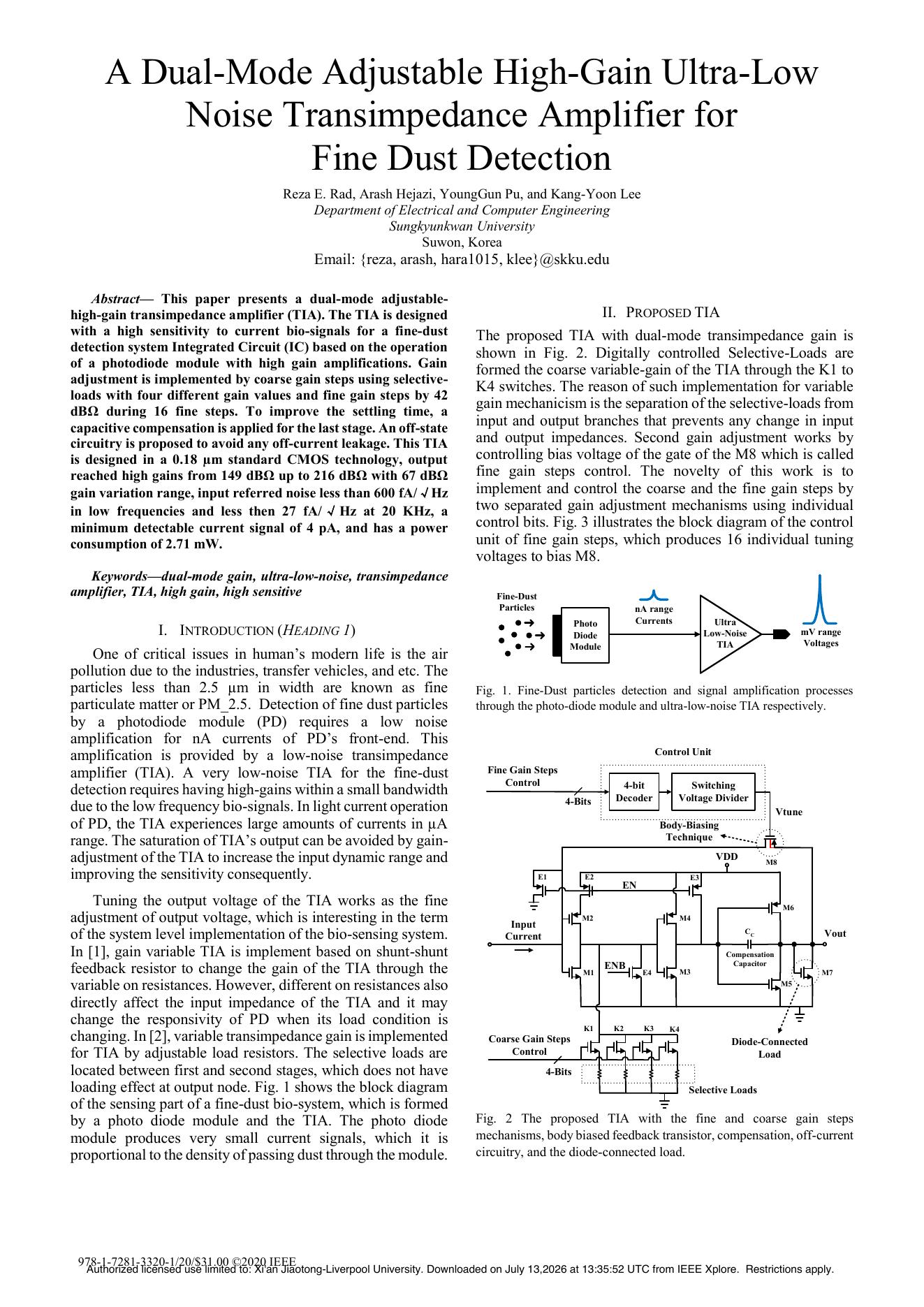
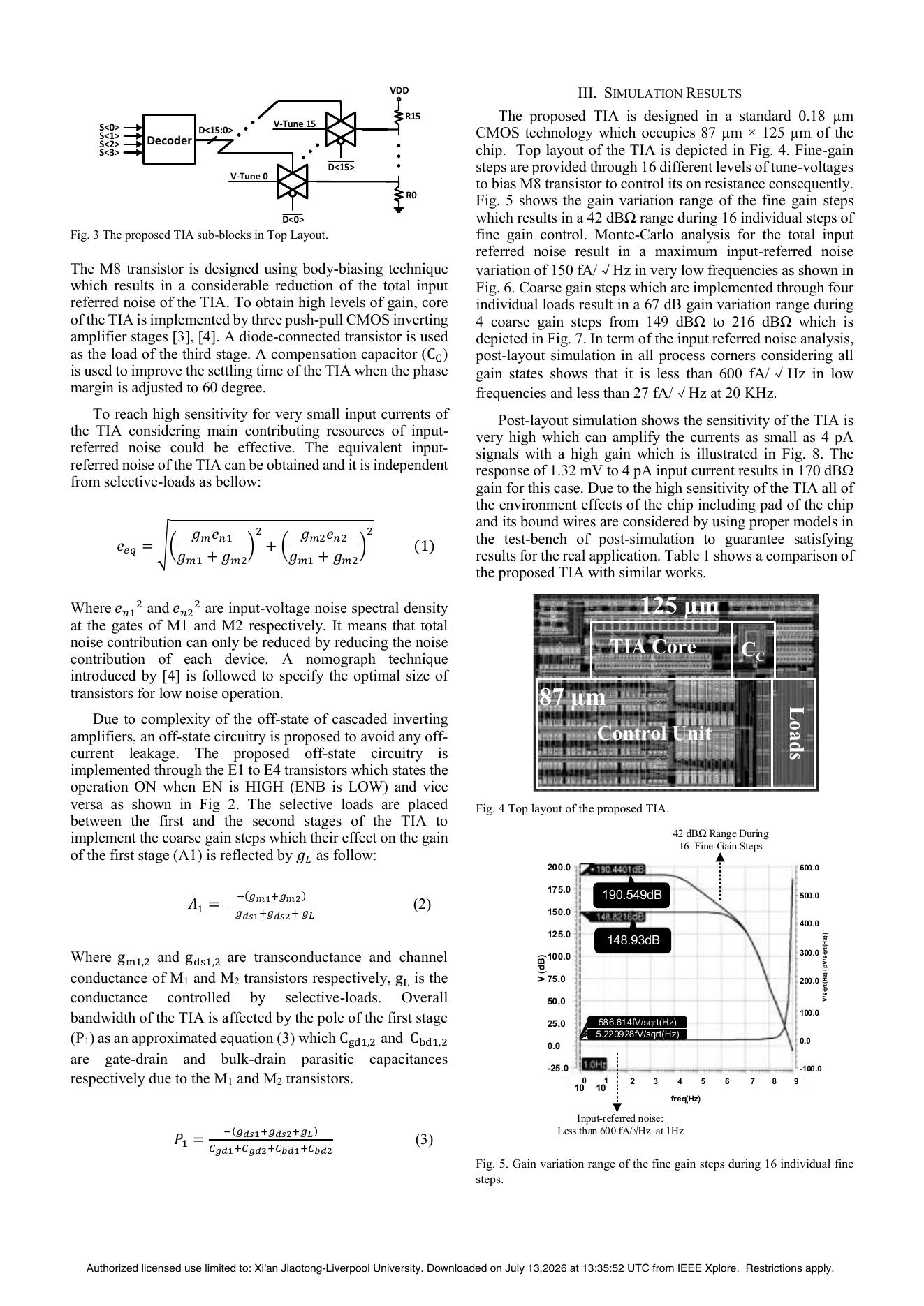
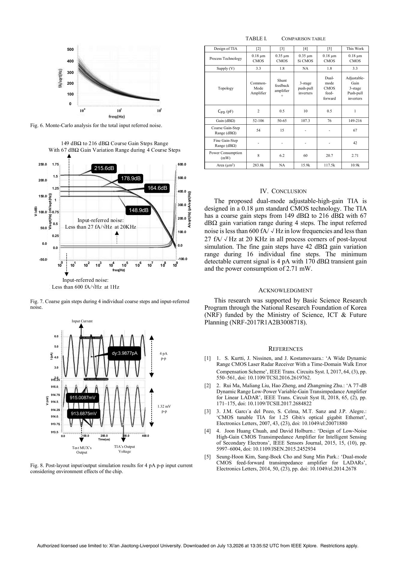
原文摘要证据:This paper presents a dual-mode adjustable- high-gain transimpedance amplifier (TIA). The TIA is designed II. PROPOSED TIA with a high sensitivity to current bio-signals for a fine-dust The proposed TIA with dual-mode transimpedance gain is detection system Integrated Circuit (IC) based on the operation shown in Fig. 2. Digitally controlled Selective-Loads are of a photodiode module with high gain amplifications. Gain formed the coarse variable-gain of the TIA through the K1 to adjustment is implemented by coarse gain steps using selective- K4 switches. The reason of such implementation for variable loads with four different gain values and fine gain steps by 42 dBΩ during 16 fine steps. To improve the settling time, a gain mechanicism is the separation of the selective-loads from capacitive compensation is applied for the last stage. An off-state input and output branches that prevents any change in input circuitry is proposed to av...
与 SOTA 对比
- 比较重点:优先比较相同输入电容、相同带宽定义和相同输出负载下的增益、噪声、线性度与功耗。
- 本文优势:可调高增益+低噪声,最贴近多阻态小电流读出
- 主要限制:优势:小电流、低噪声、可调 gain;短板:后仿,带宽需核实
- 口径提醒:会议论文中仿真值、后仿值和芯片实测值不可直接混排;未在正文报告的指标不作推算排名。
NS-RAM / CIM 适配判断
适合多阻态或不同阵列规模导致电流跨度变化的NS-RAM;需补实测噪声、带宽和增益切换稳定性后再定标。
迁移到 NS-RAM 时仍需重新确定列线电容、最小/最大读电流、允许建立时间、输出摆幅和 ADC 满量程,并据此重算反馈元件与环路稳定性。
核心优势与局限
核心优势:可调高增益+低噪声,最贴近多阻态小电流读出
主要局限:优势:小电流、低噪声、可调 gain;短板:后仿,带宽需核实
结论:该文适合作为“可调高增益低噪声 TIA:3-stage push-pull inverter + coarse/fine gain control”路线的参考,但不能脱离其原始应用和负载条件直接套用指标。
论文原图